- 您现在的位置:买卖IC网 > Sheet目录369 > W9425G6JH-5I (Winbond Electronics)IC DDR SDRAM 256MBIT 66TSOPII
�� �
�
�W9425G6JH�
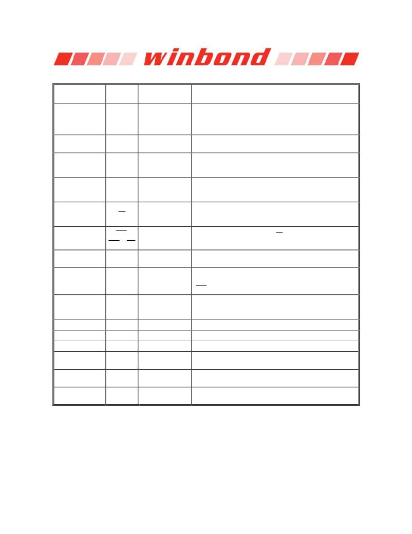
�6.� PIN� DESCRIPTION�
�PIN� NUMBER�
�28� ?� 32,�
�35� ?� 42�
�26,� 27�
�2,� 4,� 5,� 7,� 8,� 10,�
�11,� 13,� 54,� 56,� 57,�
�59, 60, 62, 63, 65�
�16,51�
�PIN�
�NAME�
�A0� ?� A12�
�BA0,� BA1�
�DQ0� ?�
�DQ15�
�LDQS,�
�UDQS�
�FUNCTION�
�Address�
�Bank� Select�
�Data� Input/� Output�
�Data� Strobe�
�DESCRIPTION�
�Multiplexed� pins� for� row� and� column� address.�
�Row� address:� A0� ?� A12.�
�Column address: A0� ?� A8. (A10 is used for Auto-precharge)�
�Select� bank� to� activate� during� row� address� latch� time,� or�
�bank� to� read/write� during� column� address� latch� time.�
�The� DQ0� –� DQ15� input� and� output� data� are� synchronized�
�with� both� edges� of� DQS.�
�DQS� is� Bi-directional� signal.� DQS� is� input� signal� during� write�
�operation� and� output� signal� during� read� operation.� It� is� Edge-�
�aligned� with� read� data,� Center-aligned� with� write� data.�
�Disable� or� enable� the� command� decoder.� When� command�
�24�
�CS�
�Chip� Select�
�decoder� is� disabled,� new� command� is� ignored� and� previous�
�operation� continues.�
�23,� 22,� 21�
�20,� 47�
�45,� 46�
�RAS� ,�
�CAS� ,� WE�
�LDM,� UDM�
�CLK� ,�
�CLK�
�Command� Inputs�
�Write� Mask�
�Differential� Clock�
�Inputs�
�Command� inputs� (along� with� CS� )� define� the� command�
�being� entered.�
�When� DM� is� asserted� “high”� in� burst� write,� the� input� data� is�
�masked.� DM� is� synchronized� with� both� edges� of� DQS.�
�All� address� and� control� input� signals� are� sampled� on� the�
�crossing� of� the� positive� edge� of� CLK� and� negative� edge� of�
�CLK� .�
�CKE� controls� the� clock� activation� and� deactivation.� When�
�44�
�CKE�
�Clock� Enable�
�CKE� is� low,� Power� Down� mode,� Suspend� mode,� or� Self�
�Refresh� mode� is� entered.�
�49�
�V� REF�
�Reference Voltage� V� REF� is� reference� voltage� for� inputs.�
�1,� 18,� 33�
�34,� 48,� 66�
�3,� 9,� 15,� 55,� 61�
�6,� 12,� 52,� 58,� 64�
�14,� 17,� 19,� 25,�
�43,� 50,� 53�
�V� DD�
�V� SS�
�V� DDQ�
�V� SSQ�
�NC�
�Power�
�Ground�
�Power� for� I/O�
�Buffer�
�Ground� for� I/O�
�Buffer�
�No� Connection�
�Power� for� logic� circuit� inside� DDR� SDRAM.�
�Ground� for� logic� circuit� inside� DDR� SDRAM.�
�Separated� power� from� V� DD� ,� used� for� output� buffer,� to�
�improve� noise.�
�Separated� ground� from� V� SS� ,� used� for� output� buffer,� to�
�improve� noise.�
�No� connection�
�Publication� Release� Date:� Aug.� 27,� 2013�
�-7-�
�Revision� A03�
�发布紧急采购,3分钟左右您将得到回复。
相关PDF资料
W947D2HBJX5E
IC LPDDR SDRAM 128MBIT 90VFBGA
W948D2FBJX5E
IC LPDDR SDRAM 256MBIT 90VFBGA
W949D2CBJX5E
IC LPDDR SDRAM 512MBIT 90VFBGA
W971GG6JB25I
IC DDR2 SDRAM 1GBIT 84WBGA
W971GG8JB-25
IC DDR2 SDRAM 1GBIT 60WBGA
W9725G6IB-25
IC DDR2-800 SDRAM 256MB 84-WBGA
W9725G6JB25I
IC DDR2 SDRAM 256MBIT 84WBGA
W9725G6KB-25I
IC DDR2 SDRAM 256MBIT 84WBGA
相关代理商/技术参数
W9425G6JH5ITR
制造商:Winbond Electronics Corp 功能描述:256M DDR SDRAM X16, 200MHZ, IN
W9425G6JH5TR
制造商:Winbond Electronics Corp 功能描述:256M DDR SDRAM X16, 200MHZ, 65
W9425G6JH-5TR
制造商:Winbond Electronics Corp 功能描述:256M DDR SDRAM X16, 200MHZ, 65
W9425G8EH
制造商:WINBOND 制造商全称:Winbond 功能描述:8M × 4 BANKS × 8 BITS DDR SDRAM
W946432AD
制造商:WINBOND 制造商全称:Winbond 功能描述:512K X 4 BANKS X 32 BITS DDR SDRAM
W9464G6IB
制造商:WINBOND 制造商全称:Winbond 功能描述:1M × 4 BANKS × 16 BITS DDR SDRAM
W9464G6IH
制造商:WINBOND 制造商全称:Winbond 功能描述:1M ?? 4 BANKS ?? 16 BITS DDR SDRAM
W9464G6JH
制造商:WINBOND 制造商全称:Winbond 功能描述:1M ? 4 BANKS ? 16 BITS DDR SDRAM